The
CBCSRK-1T Circuit Description For The Electronics
Engineers
Why do we need yet another
single transistor AM radio design? "I'm sick to death of
them," I hear you cry! They're all rubbish anyway, are
highly variable, dependant on weird properties of this and that,
use components that were last seen when dinosaurs still roamed the
Earth, and are all highly annoying in some way or other.
Bear with me on this one, and don't write into Barry Took to
complain until you've actually tried it.
PSPICE simulations do not qualify as "trying it," as PSPICE would
probably explode in a hissy fit of recursive matrices if you fed
this into it, or you'd spend more time making the models
sufficiently accurate than it actually took to build it.
The "simple" explanation provided on the main page is pretty much
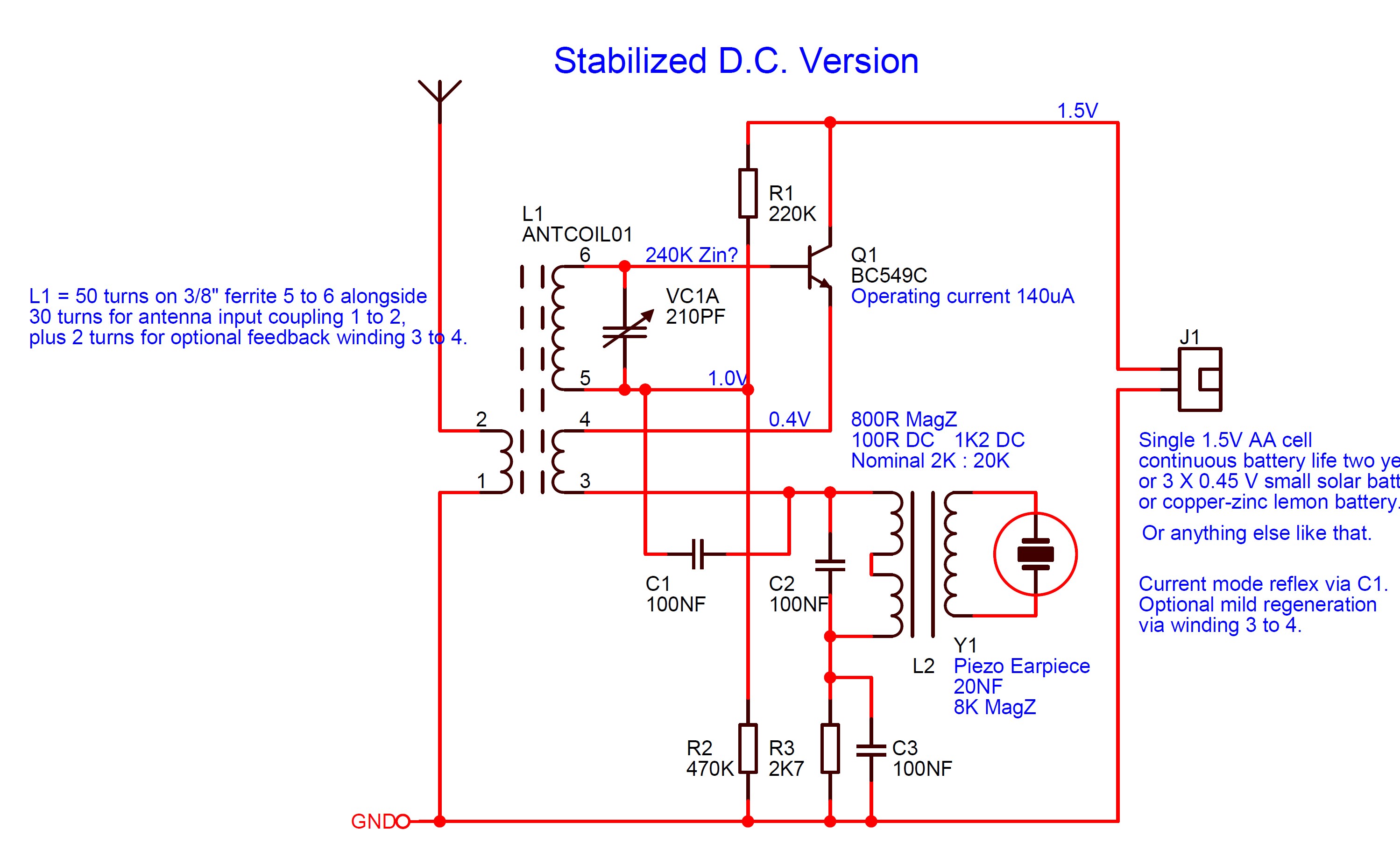
it. The aerial winding part of L1 pins 2 to 1 is straightforward.
Depending on how capacitive the aerial system is, moving the coil
away from the main resonant tank coil can improve selectivity, as
can reducing the number of turns. The arrangement shown is a good
compromise most of the time. L1 pins 6 to 5 and VC1A
comprise the resonant tuning circuit. Both sections of the
variable capacitor are used with the capacitor trimmers set to
minimum. You can tune most of MW this way, and get the rest by
moving the coil up and down on the rod. It's a, "Mr.
Slidey." The resonant tank is RF grounded at the bottom end
through C2 and C3. Then it gets kinda interesting.
Q1 is wired as an emitter follower. The idea is that the current
gain in emitter follower mode allows direct connection to the top
of the tank without damping it too much, so you get the maximum
possible voltage gain from the resonance of L1, despite getting
non at all from the emitter follower... Yet. A small
amount of initial base bias is fed through the bottom of the tank
from R1, avoiding using a DC blocking capacitor or damping the
tank with the biassing resistor. You'll see this a lot in old
transistor radios. In emitter follower mode, even a BC549C running
at low voltage can provide RF current gain at MW frequencies, so
amplified RF current comes out of the emitter. It goes through the
regen coil L1 pins 4 and 3 and is induced into the L1 system. From
this we have some RF positive feedback gain for regeneration,
without actually making any voltage gain with the transistor.
Collector-base Miller effect is non-existant.
At the top of L2, the positive current flow on RF peaks builds up
a voltage. Q1 can only flow in the positive direction, so it's
acting as an active demodulation rectifier after the regen
coil. You see that voltage across L2 primary and the
parallel capacitor. L2 is wired as a step-up transformer, and the
signal voltage gain is about 10dB. We have used the transistor in
current amplification mode and used the existing L2 transformer to
get some audio signal voltage gain.
C3 eh? In some other simple designs, you'll see a single
transistor used as a voltage amplifier, and a horrible old Clacton
Coils / Mullard transistor type radio frequency choke last seen in
1978 used to block the RF, and feed audio back to the base, where
it is indeed voltage amplified again by the same transistor doing
the RF amplification. You can see the RF riding on top of the
audio in such designs. Those particular RFCs are unobtainable,
even if you substitute a not very effective 4.7mH SMCC ferrite
inductor. A more complicated reflex feedback arrangement would use
more parts than another proper transistor stage, so would be
pointless. Here, C3 couples the audio signal from the top of L2
primary back through L1 pins 5 and 6 in a reflex bootstrap
fashion. It effectively provides more base bias for the RF peaks
and the audio signal. Q1 acting in this bootstrap mode also
effectively multiplies the values of the capacitors. 100nF is more
than sufficient. You can't see much of the RF voltage riding the
audio in this design, because it's not there. It's a current.
You may initially feel aggrieved about transistor Hfe and voltage
supply variability with the very basic bias
arrangement. Fine. Because the bias is provided
mostly by the bootstrap, once Q1 is tickled into conduction by
R1, adjustment of the amount of regeneration effectively removes
the effect of Hfe variability. The regeneration adjustment is
surprisingly stable even when tuning across the band. The
loudness limit obtainable ends up being more dependent on the
point where the circuit breaks into oscillation than the Hfe of
a particular transistor. Supply voltage variability effecting
the gain of the receiver is reduced in a similar way. The
initial quiescent current does vary with supply voltage, but the
Re of the transistor and the small DC resistance of L2 helps to
make this less critical for supply voltages between 1 and 3
Volts. Anyway, you wouldn't connect a 12V car radio to a 24V
lorry battery and expect it to survive the experience.
Oscilloscope Pictures
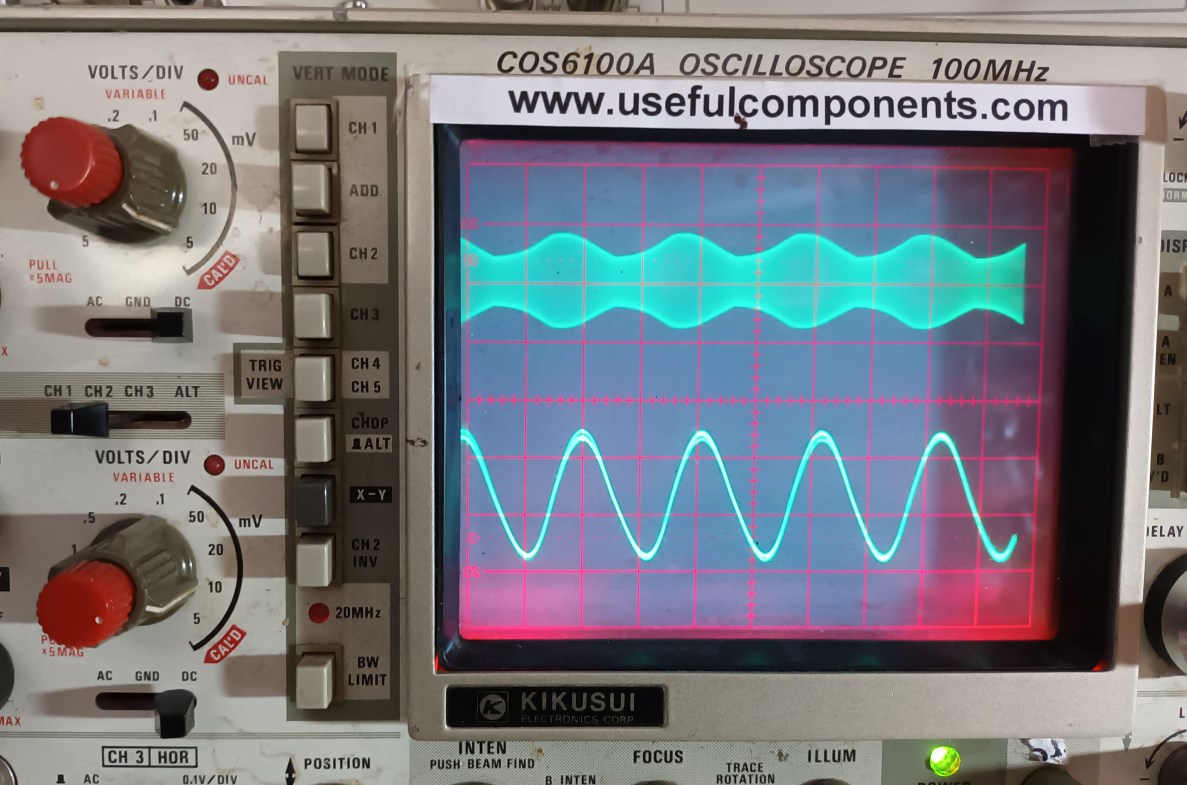
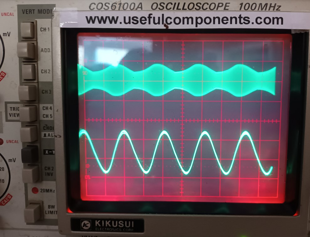
The RF voltage on Q1 base is on the upper trace and the
demodulated audio at Q1 emitter on the lower. You can just see a
bit of RF voltage on the lower trace. The upper upper trace is on
a X1 probe, the lower trace on a X10 probe, with the attenuator
settings as shown in the photograph. The signal generator is an
ancient Maplin "Precision Gold" unit set to internal 1kHz
modulation.


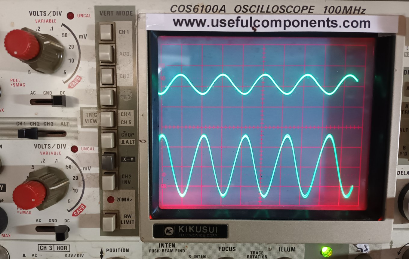
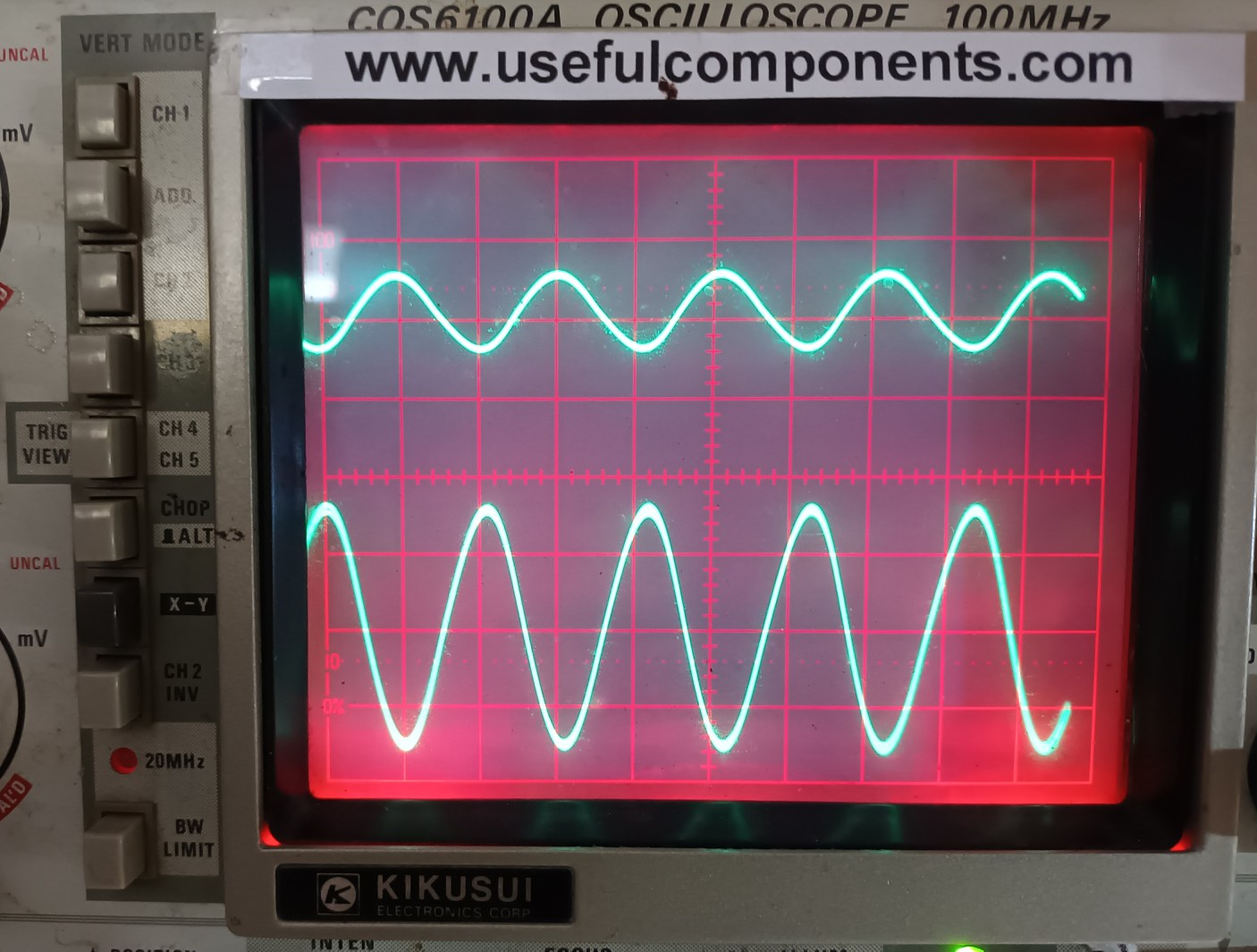
Here are the top of L2 primary and top of L2 secondary with both
probes set to X10. The voltage gain across the transformer is a
factor of 3.5, or 10.9dB. It may be possible to do better with a
higher ratio transformer, but this has worked well here. The audio
fidelity is OK, though it gets poorer with increasing
regeneration.


Current Consumption Versus Supply Voltage Table
Under the signal conditions shown above, with moderate
volume of 1kHz tone coming out of the earphone, and
moderate regeneration in action, the current consumption varies
according to the following table. You would expect to see this
vary with different transistors within the "C" gain banding, but
the low supply voltage, intrinsic emitter resistance, and L2
primary DC resistance will always keep it reasonable at the data
sheet open-ended high end.
Supply (V) Current (mA)
1.01 0.10
1.11 0.12
1.21 0.13
1.30 0.16
1.40 0.19
1.50 0.21
1.60 0.22
1.70 0.24
1.80 0.27
1.90 0.29
2.00 0.31
2.20 0.35
2.40 0.39
2.60 0.44
2.80 0.48
3.00 0.52
3.40 0.61
3.80 0.71
Not Good Enough For Yah?
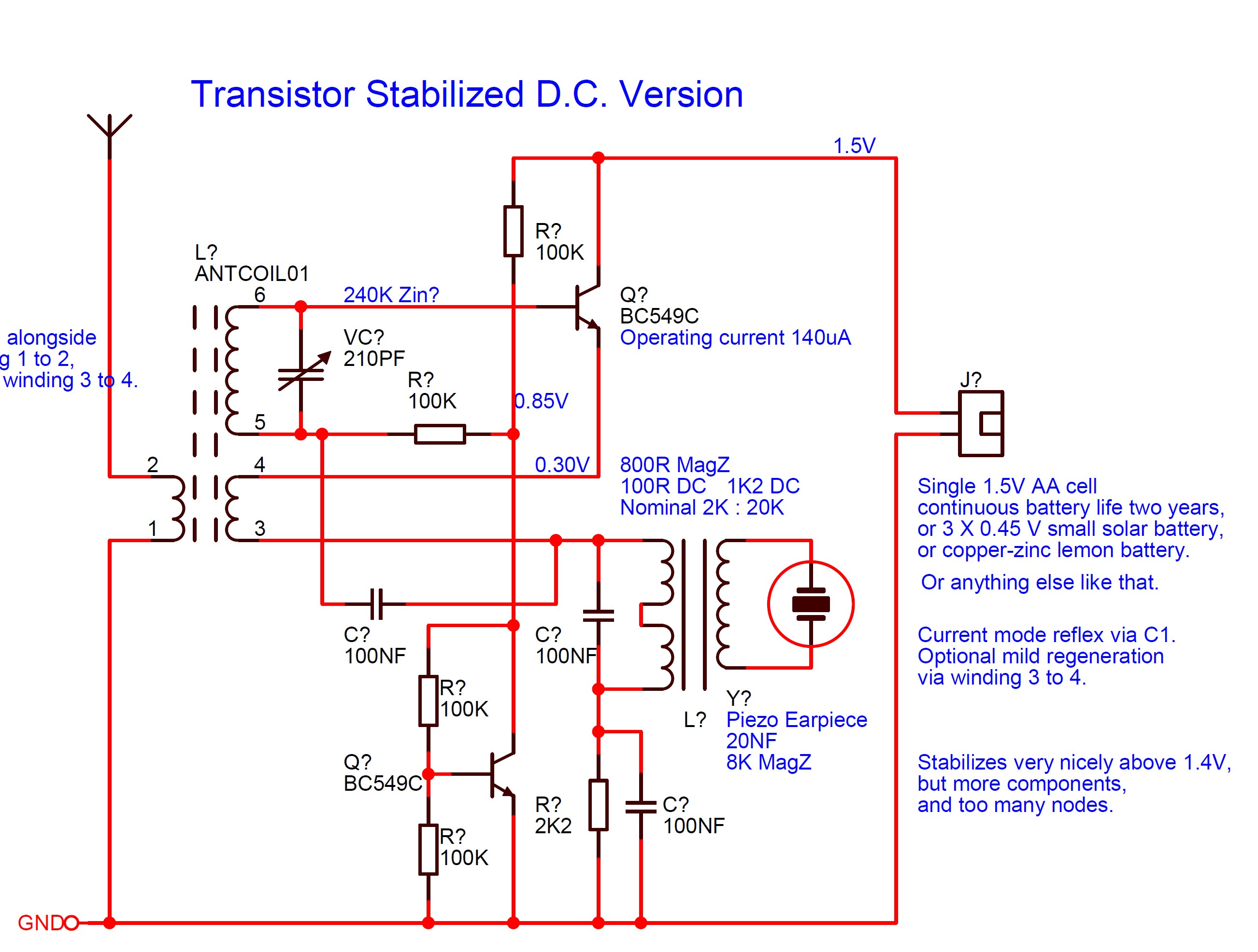
You can stabilize the quiescent current consumption quite well
using a more conventional bias arrangement, with some DC emitter
degeneration and a bypass capacitor.

Supply (V) Current (mA)
0.95 0.04
1.10 0.06
1.26 0.09
1.47 0.14
1.69 0.19
1.90 0.24
2.10 0.27
2.30 0.31
2.61 0.38
2.96 0.45
3.33 0.53
3.52 0.57
You can also stabilize the quiescent current
consumption very well up to stupidly high voltages using the nice
variable Vbe scheme seen in Horowitz and Hill.

Supply
(V) Current (mA)
1.05 0.07
1.16 0.08
1.26 0.11
1.36 0.12
1.45 0.14
1.55 0.15
1.78 0.17
1.99 0.18
2.38 0.19
2.99 0.21
Woah, Buttercup. Nice regulation, but that's looking way too
complicated, and what's the point? I had four spare holes in the
terminal strip, so there's no point getting too fancy if it
doesn't actually give the end user any more sensitivity or give
louder output. Within the boundaries of any project, it can be
better just to do the job, and to provide fewer opportunities for
failure. This applies equally as well to the marketing departments
of global high-tech mobile device manufacturers, as it does to
kids making radios.
As a final note, if you have one in your component racks, you
might want to use a TO-92 NPN Darlington transistor such as a
BC517, go up to a 3V supply, and increase R1 to about 10M
accordingly. I tried this. It works really well, even on 1.5V. I
considered using one in the kit, but I've been caught out with
obsolescence before. Obsolete parts; The electronic engineer's
nightmare. Using a BC549C or anything else like that keeps it
simple, and gives the customer an entry into the exciting world of
the transistor, with just five additional parts added to the
original kit.
Navigate Up
Have you seen a mistake? If so,
feel free to contact me at the email address below. This
address has been the same since 1997, and unless I'm on
holiday, it is checked daily including the spam folder.

Recent edit history
20-NOV-2025: Changed to direct links and self canonicalisation.
© Henry J. Walmsley 2025.
